SK Hynix moves 375-layer NAND into mass production, replacing tungsten with molybdenum
According to sources interviewed by The Elec, mass production will take place in existing fabs, which currently produce 321-layer V9 NAND. Inside the company, the 375-layer design has been referred to as a "400-layer" product. Read Entire Article
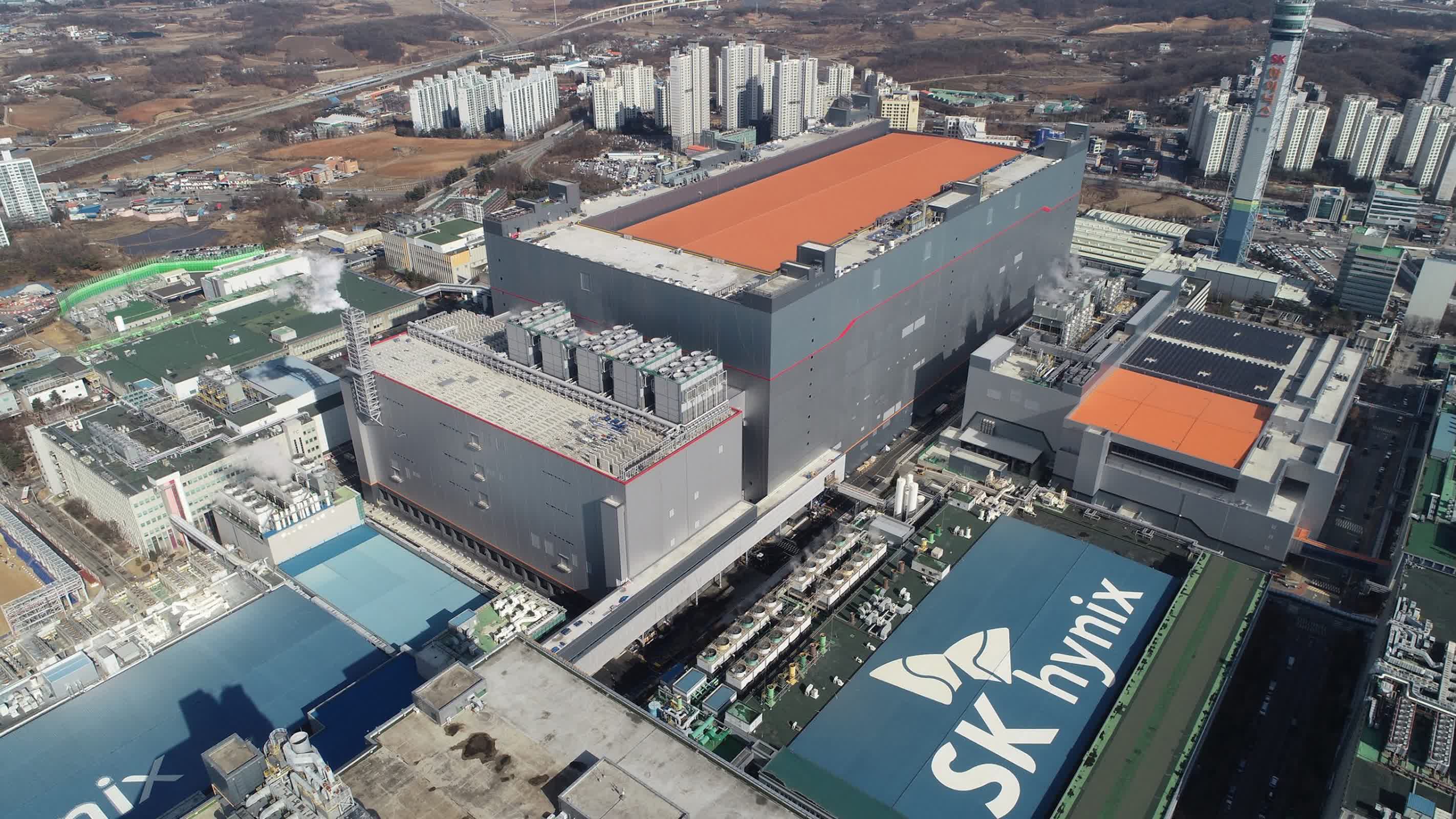
Rumor mill: SK Hynix is moving closer to its next step in NAND scaling, with plans to bring its 375-layer flash memory into mass production by the end of 2026. The company has already completed verification, clearing a key hurdle before volume production. The move marks progress in vertical memory design and also points to the limits of increasing layer counts. According to sources interviewed by The Elec, mass production will take place in existing fabs, which currently produce 321-layer V9 NAND. Inside the company, the 375-layer design has been referred to as a "400-layer" product. The difference reflects a basic problem in high-layer NAND: beyond a certain point, simply adding more layers becomes difficult with current methods. As stacks grow taller, keeping the electrical connections reliable gets harder, and companies may have to sacrifice some layers to protect yield and performance. Those limits are also affecting SK Hynix's longer-term plans. The company has future NAND generations in development with 480 and 604 layers, but getting there will require more than incremental improvements. One of the most significant changes under consideration is a shift in materials. The company plans to replace its current tungsten film with molybdenum. Tungsten has long been a standard material in NAND manufacturing, but it becomes less effective as wiring narrows and resistance increases. At higher layer counts, that resistance can interfere with signal transmission across the chip. Molybdenum offers better electrical characteristics under these conditions and is already being used by Samsung in its own advanced NAND designs. This shift shows how NAND scaling is evolving. Adding more layers is still the goal, but the bottleneck is increasingly about how well signals can move through a densely packed vertical structure. Materials, in other words, are becoming just as important as architecture. Competition is also playing a role in how quickly these changes are happening. Samsung is pushing beyond 400 layers with its own roadmap and is working toward much higher counts using dual-stacking approaches. The company is expected to roll out its first 400-layer V-NAND products soon, keeping pressure on SK Hynix as both chip giants try to outpace each other in density and performance. The ripple effects are already showing up in the supply chain. Demand for molybdenum is climbing as manufacturers prepare for the next wave of NAND production. Samsung reportedly bought 4 tons of the material last year and has already secured 10 tons this year. SK Hynix is expected to use around 4 tons as it ramps up. Industry estimates put demand at 25 tons in 2027, 40 tons in 2028, 60 tons in 2029, and 80 tons by 2030. That kind of growth shows how central new materials are becoming to the future of memory manufacturing.
Comments
No comments yet. Start the discussion.