Teardown: The BMW / Harman IDC23H Infotainment Unit (B423)
Overview
Another day, another teardown - and the first blog post of 2026! Today we’ll be looking at the BMW IDC23H infotainment unit, manufactured by Harman Becker. The IDC23H is one of the newest infotainment units from BMW, as of January 2026. The design is based on the previous-generation MGU22/MGU22H, and is used in a wide variety of BMW models - this unit in particular was found in one of BMW’s newest X1 U11 SUVs.
While previous generations of BMW infotainment unit were primarily developed by Harman Becker themselves, this unit appears to be a joint venture between both Harman Becker and Garmin - similar to the MGU22 units. The design is sold under two different names:
- IDC23 (produced by Garmin)
- IDC23H (produced by Harman Becker)
This naming scheme was the same in the prior MGU22 lineup, where the MGU22 was produced by Garmin, and the MGU22H was produced by Harman. Essentially, it seems that ‘H’ at the end of the model name = Harman.
As for connectivity, this unit provides the following:
- APIX connectivity to the Driver Camera System (DCS)
- APIX connectivity to the Heads-Up Display (HUD)
- APIX connectivity to the Driver’s Display (DFE)
- 2.4GHz/5GHz WiFi Connectivity WLAN 802.11 abgn/ac/ax MIMO 2x2
- Bluetooth EDR/BT 5.0 connectivity
- Navigation satellite connectivity (GNSS)
- 100BASE-T1 Ethernet
- 1GBASE-T1 Ethernet
- AR-CAM Connectivity
- APIX connectivity to the Central Information Display (CID)
- 1-3x USB Connectivity
This system presents a few interesting new pieces of connectivity I haven’t seen on previous versions of BMW’s infotainment! Of particular interest to me are the DCS and DFE connections. According to the documentation I could find, the new Driver Camera System “detects the alignment of the driver’s head and their line of sight. This is required for the ‘Fatigue Alert’ function.” As for the DFE connection, it may seem boring at first sight: it just connects to the driver’s display, right? Well, that “driver’s display” is actually the vehicle’s instrument cluster. This means on the newest generation of vehicles, BMW appears to have fully removed the dedicated “KOMBI” instrument cluster module, instead relying on the head unit to drive both the instrument cluster and infotainment systems!
Overall, some cool new changes to the latest system. I’m sure this will make people want to hack and modify the unit all the more, as they want custom boot animations and skins on their instrument cluster and whatnot :)
Basic Specs
Before we dive into the full detailed teardown, let’s go over the basic system specs:
- Main Processor: Qualcomm Snapdragon SA8155P
- RAM: 12GB of LPDDR4
- Interface Processor: Infineon “TRAVEO” CYT3BB-series ARM Cortex M7F
- Storage: 128 GB of UFS v3.1
The Outside of the Unit
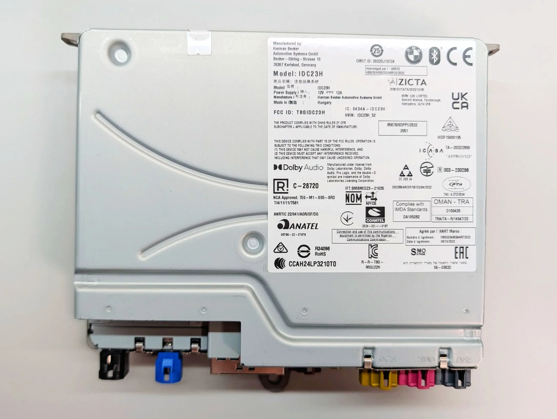
The outside of the unit is relatively standard, with a rectangular design reminiscent of the previous generation BMW MGU22 infotainment system. Labels are affixed to the top and front of the unit, and the device’s numerous I/O ports are scattered across the rear. The left and right side feature holes for ventilation, and the underside of the unit is made of a thick metal, acting as a heatsink for the underside of the PCB inside.
Top Label Information
The top label features many useful pieces of information about the device:
- Manufactured by: Harman Becker Automotive Systems GmbH
- Model: IDC23H
- FCC ID: T8GIDC23H
The full text dump of the top label information can be found in the Appendix section at the bottom of this post.
Front Label Information
The device’s front label also features many key pieces of information, including the device’s part number and manufacturing date:
- Model: IDC23H
- EC: 202
- SPN: 4165630
- Type-Nr.: HB B423
- Date: 31/24
- HWEL: 5.2.1
- BMW GROUP 6512 CI 5B67397 01
Converting that final number into a BMW part number, we get: 65125B67397. Unfortunately, I haven’t been able to find any hits for this part number - it’s possible the part number is from a vehicle too new to be in BMW’s parts system yet. As with the top label, the full text dump of the front label can also be found in the Appendix section at the bottom of this post.
The Rear Side & I/O
Around the rear, we can take a closer look at the I/O. Starting from the left, we first have the black BT/WLAN connector. Then, USB 1/2/3, though this device only features a single blue connector in the “USB 2” slot. The large black connector to its right is labeled “MAIN”, and is the main wiring harness connector to the vehicle. To the right of the MAIN connector, the red connector is labeled “CID” and connects to the vehicle’s Central Information Display. Next is the brown “AR-CAM” connector, which helps facilitate BMW’s new Augmented Reality camera navigation functionality. Finally, on the far right side, we have a pair of Ethernet ports on the bottom - the white port being 100BASE-T1, and the black port being 1GBASE-T1. Above those we have three additional display connectors, labeled “DCS” (brown connector) for the Driver Camera System, “HUD” (pink connector) for the Heads Up Display, and “DFE” (gray connector) for the driver’s display.
The Inside
Popping the lid, we get our first look at the inside of the device. Honestly, it’s exceedingly similar to the previous-generation MGU22! But we have a few sparkly new changes, starting with the new APIX connectivity PCB that holds the DCS, HUD, and DFE connectors. This unit is only made up of two PCBs, which I’ll refer to as:
- The main device PCB
- The APIX connectivity PCB
Now then, let’s dive in!
APIX Connectivity PCB
PCB Label: GARMIN 105-04748-00 VER 1 HWVER5.2.1
The APIX connectivity PCB is the biggest new addition from the old MGU22 unit’s design! This small PCB appears to exist for facilitating additional APIX video streaming connectivity with a number of other devices in the vehicle - in this case, the Driver Camera System (DCS), Heads Up Display (HUD), and DFE systems. The stars of the show on this PCB are the two large Inova APiX 3 ICs, and their associated trio of connectors. The underside of the PCB holds a large connector for facilitating connectivity between this small board and the device’s main PCB. If I counted correctly, this connector has 100 total pins (50 per side) and features an “HRS” logo, pointing to the manufacturer being HIROSE, a well-established supplier of high quality connectors. Interestingly, if the silkscreen labeling is to be believed, this small board is actually a six layer PCB! That’s quite a lot of complexity packed into such a small board.
Major Components - APIX PCB
- Inova Semiconductors APiX 3 Transmitters (x2) (datasheet)
INAP565TAQ 37140_2415 - Analog Devices MAX916714F GMSL2/GMSL1 to CSI-2 Deserializer (datasheet)
96714FG TJ/VY 2351 +babd
And on the underside of the board:
- Texas Instruments 2HB16BQ Dual-Channel Smart High-Side Power Switch (datasheet)
43TE4 ATS3
Main Device PCB
PCB Label: GARMIN 105-04747-00 VER 3 HWVER 5.2.1
After removing the APIX PCB, we can see the device’s main PCB. An impressively large active cooling system occupies the left side of the board, with the right half being dedicated mainly to the APIX connector PCB. Interestingly, it seems like the provisions for a second 100-pin connector exist at the top of the board, with another 100 pads unpopulated. Perhaps this is for future revisions of the board, or a second daughter board that was scrapped during the development process. To get a closer look at the rest of the PCB, we’ll first have to deal with removing the heat sink. It’s quite beefy, and uses a Delta Electronics brush-less fan to force air over the cooling fins in a design that reminds me a lot of a laptop cooling heat sink. The heat sink is relatively easy to remove - just a few screws and a bit of thermal compound to deal with.
Moving the heat sink aside, we get to the heart of the module: A Qualcomm Snapdragon SA8155P module, an Infineon CYT3BB microcontroller, and 128 GB of Micron UFS v3.1 storage. Because the Qualcomm module has its own little BGA PCB, I’ll also list the silkscreen markings here: GARMIN 105-04129-11 VER 1 4021519 AT&S MX6 SH 2024
Operating System & Architecture Guesses
Unfortunately, I haven’t been able to dive into this unit’s operating system quite yet - I’m still waiting on some adapters to arrive so I can try dumping the UFS storage. More blog posts to come! As for the device’s overall architecture, it’s likely similar to prior Harman units. My guess is that the Qualcomm processor is responsible for the ‘higher level’ video processing and application functionality, while the Infineon is likely responsible for lower-level tasks like CAN communications with the rest of the vehicle. This is also supported by the Infineon IC’s datasheet, which notes this specific chip has 8 CAN FD channels, 16 LIN channels, and one 10/100 Mbps Ethernet interface built-in.
Main Device PCB (Underside)
Flipping to the back side of the PCB, we can see many of the “supporting” ICs for various bits of device functionality - an Ethernet switch, another APiX 3 IC, an NXP WiFi/Bluetooth transceiver, and a few other small ICs dotted around the board. The specific IDC23H I have unfortunately doesn’t contain a GNSS transceiver, but according to this FCC document, models that do feature GPS/GNSS likely use the Ublox UBX-M8030.
Major Components - Main Device PCB (Top Side)
- Qualcomm Snapdragon SA8155P Microcontroller Module (datasheet)
- Qualcomm Power Management ICs (x2) (listed on main 8155P datasheet)
These power management ICs appear to be specific to the SA8155P platform.
Apologies for the wacky photo - they were extremely hard to photograph, so I ended up using some isopropyl alcohol as a makeshift lens to increase clarity, haha.
PMM8155AU 002-01 PE415BXF - Micron 2133MHz LPDDR4 RAM (6GB x2) (catalog listing)
I think these modules are 6GB each in size (giving the unit 12GB of RAM in total), but the datasheet for this RAM is currently completely unavailable without a Micron account.
41C77 D8DCZ B9JF MT53E1536M32D4DE-046 AIT:C - Infineon “TRAVEO” CYT3BB-series ARM Cortex M7F Microcontroller (datasheet)
CYT3BB8CEBQ0AES GS 415VV015 B 10 CYP TWN C - Micron 128GB UFS 3.1 Storage (catalog listing)
4CA22 AM022 MTFC128GBCAVTC-AIT
Major Components - Main Device PCB (Underside)
- Marvell 8-port Automotive Ethernet Switch (datasheet)
Apparently this switch features Deep Packet Inspection (DPI) functionality, which I found surprising!
88Q5050-LKJ2 P34B57B.05 2348 B0P TW - Inova Semiconductors APiX 3 Transmitter (datasheet)
This APiX 3 IC is actually a higher-end model than those used on the APIX-specific daughterboard, being a “596” model, as opposed to the pair of lower-spec “565” models used on the daughterboard. Its main ‘killer feature’ is the addition of HDCP protocol support, allowing the Central Information Display to play DRM-protected video content.
INAP596TAQ 33182-2410 - Texas Instruments LVDS Deserializer (datasheet)
UB936Q TI 43I AE03 G4 - NXP 2.4/5 GHz Dual-Band WiFi 6 + Bluetooth 5.3 SoC (datasheet)
88Q9098-NYB2 TMP677.25 Y0nD2408A2 A063 - Marvell / Infineon BRIGHTLANE Automotive 1000Base-T1 PHY (datasheet)
Q2221MNVA P3BM58A02 2347 B0P TW G1 - Texas Instruments Dual-Channel Smart High-Side Power Switch (datasheet)
1HB16BQ 44TE4 AT5Y - NXP CAN-FD Transceiver (datasheet)
T1145A GL9J1AC - Texas Instruments DC-DC Buck Controller (datasheet)
LM25143Q RHARQ1 TI A0438 AX1D G4
Conclusion & Closing Thoughts
This was a fun device to perform a teardown of, and I’m excited to dive into the device’s actual OS more in the future. I’m also hoping to pick up an MGU22H in the future for a more in-depth side-by-side comparison! Now the next question is… can it run DOOM? 🤔
As always, thanks for reading, and happy hacking! (Oh, and as a small bonus for reaching the end, I’ve included a modified and wallpaper-ized version of the header image below. I hope someone enjoys it! haha.)
Appendix
The appendix holds all supplementary information or references that didn’t have a home in the main portion of the article. I’ve included full raw text dumps of the top and front label data, along with other misc. links to info about the device (such as FCC information).
Yellow color used for headings and highlights: #ffd300
Similarities With the MGU22H
Now, those of you who are already familiar with the previous generation BMW head unit (the MGU22, or MGU22H) may have already noticed: This thing is extremely similar! If someone asked me to describe the IDC23H in one sentence, my answer would be “MGU22H + APIX board”. I made a side-by-side comparison of the two device’s PCBs to highlight some of the differences:
I’ve circled the few small changes that I can spot between the two devices, but most could even boil down to individual region or trim differences (ie: DAB support vs SDARS, the addition of multiple USB ports, etc.). The biggest difference between the two boards (that I can spot) is the new 100-pin connector for attaching the APIX PCB.
Now, I’ll also add the caveat that these are probably very different hardware revisions, so different hardware revisions or region boards may have different connectors or features. But it’s safe to say that the IDC23’s design is heavily based on the MGU22’s.
Acronym Adventures: DFE = ???
The new APIX board present on the IDC23H has three connections on it:
- DCS - Brown Connector
- HUD - Pink Connector
- DFE - Gray Connector
The first two, the DCS and HUD, were easy enough to figure out - DCS stands for Driver Camera System, which is part of BMW’s new fatigue alert monitoring system. HUD stands for Heads Up Display, which is the heads-up display which is projected onto the vehicle’s windscreen. But the last connector, DFE, was messing with me! What in the world could DFE stand for? I’ve done a bit of research and found documentation that stated the gray connector attaches to the “driver’s display”, but I couldn’t find any definitions for the acronym “DFE”. It appears the “driver’s display” is specifically the left-most side of the “display
Comments
No comments yet. Start the discussion.