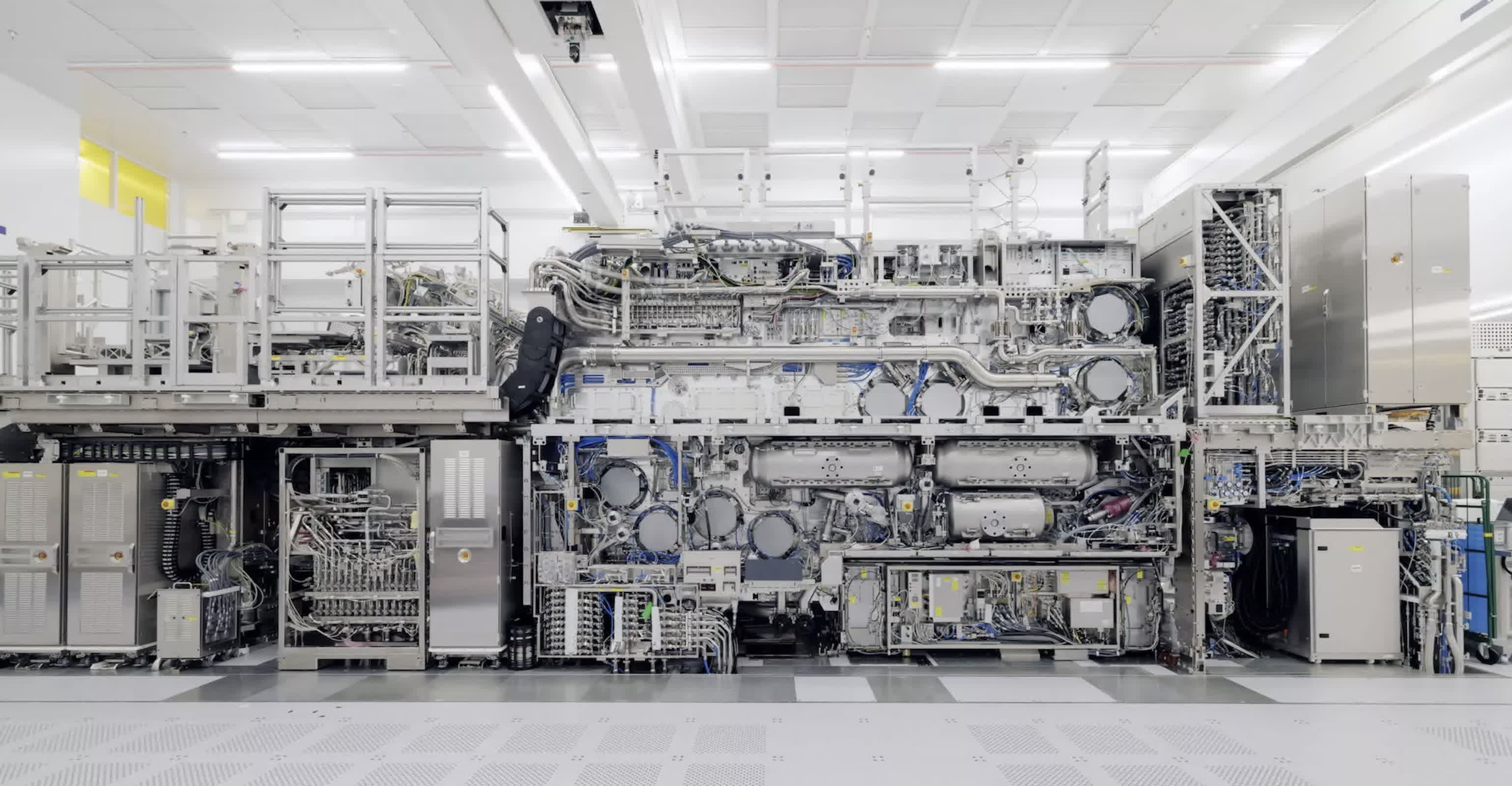
ASML targets 2033 for High-NA EUV with larger masks, promising a 40% productivity gain
High-NA EUV is ASML's next major lithography platform. It can print finer features than today's EUV tools, which could help chipmakers build denser designs at advanced nodes. But its smaller mask limits the die area that can be printed in one exposure.
Larger mask format
ASML is working with customers on a larger mask format for its next-generation High-NA EUV lithography tools, a change that could make the systems more useful for the biggest AI and data center chips. The company's current EUV machines can print chips measuring up to about 800 square millimeters. That's large enough for processors and accelerators designed by Nvidia, Google, and other companies building advanced data center hardware.
ASML now plans to move to a 12-inch mask format for High-NA EUV. The larger mask would allow the new machines to handle chips as large as the biggest data center devices made with existing EUV equipment.
Lithography tools print circuit patterns onto silicon wafers by shining light through a mask containing the chip design. The mask size determines how much of that design can be exposed at once. For makers of large GPUs, AI accelerators, and custom cloud chips, that limit is important. Many of those processors are designed close to the maximum die size that can be manufactured economically.
Timeline and production plans
- ASML expects to show a pilot line using the larger masks in 2031
- Plans to have the technology ready for high-volume production by 2033
- The company said it will need cooperation from customers and other industry participants to make the transition work
Intel is already using ASML's High-NA systems for laptop chips. TSMC and Samsung, however, have not yet deployed the equipment in high-volume manufacturing for logic chips.
Industry adoption schedules
- SK Hynix: considering whether to join the consortium working on introducing 12-inch masks; targeting 2028 for High-NA EUV in mass production of DRAM chips
- Samsung: plans to begin using High-NA EUV for high-volume DRAM production in 2028
- TSMC: expects to introduce the technology in high-volume manufacturing of advanced-node chips starting in 2030
The schedules show that High-NA EUV is moving from early use into broader production planning.
Productivity and cost
"If we're going to pull it off as an industry, then you'll actually see that the productivity of those systems will go up by 40%," ASML Chief Technology Officer Marco Pieters told Reuters.
The effort is meant to broaden the appeal of High-NA EUV, which is expected to be more expensive and more technically demanding than the current generation of EUV equipment. The machines offer improved resolution, but chipmakers also need enough wafer output to justify using them in volume production.
ASML's work on larger masks would address a separate problem: ensuring the technology can support the oversized chips increasingly used for AI systems and cloud infrastructure.
Comments
No comments yet. Start the discussion.